Quantcast
Channel: University of Cambridge - Department of Physics
Viewing all 258 articles
Browse latest View live

Diamond ‘flaws’ pave way for nanoscale MRI

$
0
0

By exploiting flaws in miniscule diamond fragments, researchers say they have achieved enough coherence of the magnetic moment inherent in these defects to harness their potential for precise quantum sensors in a material that is 'biocompatible'.

Nanoscopic thermal and magnetic field detectors - which can be inserted into living cells - could enhance our understanding of everything from chemical reactions within single cells to signalling in neural networks and the origin of magnetism in novel materials.

Atomic impurities in natural diamond structure give rise to the colour seen in rare and coveted pink, blue and yellow diamond. But these impurities are also a major research focus in emerging areas of quantum physics.

One such defect, the Nitrogen-vacancy Centre (NVC), consists of a gap in the crystal lattice next to a nitrogen atom. This system tightly traps electrons whose spin states can be manipulated with extreme precision.

Electron coherence - the extent to which the spins of these particles can sustain their quantum mechanical properties - has been achieved to high levels in the NVCs of large 'bulk' diamonds, with coherence times of an entire second in certain conditions - the longest yet seen in any solid material.

However in nanodiamonds - nanometer sized crystals that can be produced by milling conventional diamond - any acceptable degree of coherence has, until now, proved elusive.

Nanodiamonds offer the potential for both extraordinarily precise resolution, as they can be positioned at the nano-scale, and biocompatibility - as they have can be inserted into living cells. But without high levels of coherence in their NVCs to carry information, these unique nanodiamond benefits cannot be utilised.

By observing the spin dynamics in nanodiamond NVCs, researchers at Cambridge's Cavendish Laboratory, have now identified that it is the concentration of nitrogen impurities that impacts coherence rather than interactions with spins on the crystal surface.

By controlling the dynamics of these nitrogen impurities separately, they have increased NVC coherence times to a record 0.07 milliseconds longer than any previous report, an order of significant magnitude - putting nanodiamonds back in play as an extremely promising material for quantum sensing.

The results are published today in the journal Nature Materials.

"Our results unleash the potential of the smallest magnetic field and temperature detector in the world. Nanodiamond NVCs can sense the change of such features within a few tens of nanometres - no other sensor has ever had this spatial resolution under ambient conditions," said Helena Knowles, a researcher on the study.

"We now have both high spin coherence and spatial resolution, crucial for various quantum technologies."

Dr Dhiren Kara, who also worked on the study, points out that the nanodiamond's biocompatibility can provide non-invasive optical access to magnetic changes within a living cell - essentially the ability to perform MRI and detect, for instance, a cell's reaction to a drug in real time.

"We may also be able to answer some key questions in material science, such as magnetic ordering at the edges of graphene or the origin of magnetism in oxide materials," Kara said.

Dr Mete Atature, director of the research, added: "The pursuit of simultaneous high NVC coherence and high spatial resolution, and the fact that nanodiamonds couldn't deliver on this promise until now, has required researchers to invest in alternative means including advanced nanofabrication techniques, which tends to be both expensive and low-yield."

"The simplest solution - feasible and inexpensive - was in front of us the whole time."

Breakthrough offers high-sensitivity nanoscale sensors, and could lead to magnetic imaging of neuron activity and thermometry on a single living cell.

The simplest solution - feasible and inexpensive - was in front of us the whole time
Mete Atature
Nanodiamonds

This work is licensed under a Creative Commons Licence. If you use this content on your site please link back to this page.

Yes
News type: 

Quantum waves at the heart of organic solar cells

$
0
0

By using an ultrafast camera, scientists say they have observed the very first instants following the absorption of light into artificial yet organic nanostructures and found that charges not only formed rapidly but also separated very quickly over long distances - phenomena that occur due to the wavelike nature of electrons which are governed by fundamental laws of quantum mechanics.

This result surprised scientists as such phenomena were believed to be limited to "perfect" - and expensive - inorganic structures; rather than the soft, flexible organic material believed by many to be the key to cheap, 'roll-to-roll' solar cells that could be printed at room temperatures - a very different world from the traditional but costly processing of current silicon technologies.

The study, published today in the journal Science, sheds new light on the mystery mechanism that allows positive and negative charges to be separated efficiently - a critical question that continues to puzzle scientists - and takes researchers a step closer to effectively mimicking the highly efficient ability to harvest sunlight and convert into energy, namely photosynthesis, which the natural world evolved over the course of millennia.

"This is a very surprising result. Such quantum phenomena are usually confined to perfect crystals of inorganic semiconductors, and one does not expect to see such effects in organic molecules - which are very disordered and tend to resemble a plate of cooked spaghetti rather than a crystal," said Dr Simon Gélinas, from Cambridge's Cavendish Laboratory, who led the research with colleagues from Cambridge as well as the University of California in Santa Barbara.

During the first few femtoseconds (one millionth of one billionth of a second) each charge spreads itself over multiple molecules rather than being localised to a single one. This phenomenon, known as spatial coherence, allows a charge to travel very quickly over several nanometres and escape from its oppositely charged partner - an initial step which seems to be the key to generating long-lived charges, say the researchers. This can then be used to generate electricity or for chemical reactions.

By carefully engineering the way molecules pack together, the team found that it was possible to tune the spatial coherence and to amplify - or reduce - this long-range separation. "Perhaps most importantly the results suggest that because the process is so fast it is also energy efficient, which could result in more energy out of the solar cell," said Dr Akshay Rao, a co-author on the study from the Cavendish Laboratory.

Dr Alex Chin, who led the theoretical part of the project, added that, if you look beyond the implications of the study for organic solar cells, this is a clear demonstration of "how fundamental quantum-mechanical processes, such as coherence, play a crucial role in disordered organic and biological systems and can be harnessed in new quantum technologies".

The work at Cambridge forms part of a broader initiative to harness high tech knowledge in the physics sciences to tackle global challenges such as climate change and renewable energy. This initiative is backed by both the UK Engineering and Physical Sciences Research Council (EPSRC) and the Cambridge Winton Programme for the Physics of Sustainability. The work at the University of California in Santa Barbara was supported by the Center for Energy Efficient Materials, an Energy Frontier Research Center funded by the U.S. Department of Energy, Office of Science, Basic Energy Sciences under Award #DC0001009.

Researchers have been able to tune ‘coherence’ in organic nanostructures due to the surprise discovery of wavelike electrons in organic materials, revealing the key to generating “long-lived charges” in organic solar cells - material that could revolutionise solar energy.

One does not expect to see such effects in organic molecules - which [...] tend to resemble a plate of cooked spaghetti
Simon Gélinas
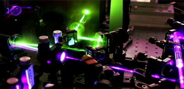
This is the experimental setup used to generate femtosecond laser pulses which serve as an ultrafast "flash " for the camera so that very rapid phenomenon can be filmed

This work is licensed under a Creative Commons Licence. If you use this content on your site please link back to this page.

Yes
News type: 

Understanding the chain fountain - a problem-solving partnership

$
0
0

The problem of the chain fountain was revealed by BBC Science presenter Steve Mould. 2.8 million people have watched his video demonstration of a chain appearing to defy gravity by first leaping out of a pot before falling to the ground. 

Professor Mark Warner and Dr John Biggins have published the first formal explanation of the physics behind this puzzle in Proceedings of the Royal Society A

Alongside this paper, the Rutherford Schools Physics Partnership has published a collection of problems which take sixth-form scientists from their AS knowledge to an explanation of the research problem. The collection is available on the RSPP on-line learning platform.

“This is a unique opportunity,” explained Professor Warner. “Because physics is such a linear subject, it normally takes years to build up to tackling a research problem like this one.”

“The key insight into the chain fountain is that, if you pick a chain up from a table, as well as you pulling the chain into motion the table must also push.  Only then can you get a fountain at all.  The whole question of the rise relates to fundamentals of momentum conservation along with energy balance.  It relates to a wide class of such problems in nature and in technology.”

“For the problem of the chain fountain, the Rutherford School Physics Partnership has been able to publish a collection of problems which, when worked through, will take young people from the simple statics of chains to the model which predicts how high the fountain should rise.”

“We hope that by showing how the problems studied at school relate to real academic challenges, young people will develop confidence in their ability to solve physics problems and be inspired to continue studying physics to a higher level.”

The Rutherford School Physics Partnership is a project designed to offer support and extension activities in physics problem solving to teachers and students transitioning from GCSE (Y11), through to Sixth Form (Y12 & 13), through to university, by combining an on-line study tool with face-to-face events at partner schools and institutions across the UK.

“We will be looking to exploit the surprises that Steve Mould revealed in a much wider range of problems that we are working on,” added Dr Biggins.

“We hope that the young people taking part in the Rutherford Schools Physics Partnership will be working on them alongside us.”

Teachers are invited to join Professor Warner and Rutherford Physics Project colleagues for a free annual residential event which in 2014 will run from the 28th – 30th June 2014.  To assist with supply cover costs, teachers from state schools may apply for a grant to cover the final Monday of the residential.  For further information see http://www.rutherford-physics.org.uk/

For Y12 students there will also be a residential event in Cambridge as part of the Project from the 29th June – 3rd July 2014 and information can be found at http://www.rutherford-physics.org.uk/

  • A podcast in which Professor Warner and Dr Biggins explain the physics of the chain fountain is available here.

The Rutherford School Physics Partnership is giving A-level physicists a unique opportunity to tackle a real research problem.

We hope that by showing how the problems studied at school relate to real academic challenges, young people will develop confidence in their ability to solve physics problems and be inspired to continue studying physics to a higher level.
Professor Mark Warner

This work is licensed under a Creative Commons Licence. If you use this content on your site please link back to this page.

Yes
News type: 

Cambridge scientists honoured in Top 100

$
0
0

Science today is not only about the work of academics and researchers: it relies on a broad spectrum of dedicated people – teachers and mentors, policy makers and regulators, writers and broadcasters, business entrepreneurs and product developers.

A Science Council initiative, aimed at recognising the many heroes of science, includes nine Cambridge scientists in its list of the top 100 people.

Science Council chief executive Diana Garnham said: “Science is like an orchestra. It takes many instruments working together to produce a fine performance. At the moment, almost exclusively, it is the virtuosity of the soloists being addressed and praised. It is vital that this narrow vision is challenged urgently because it is inhibiting education policy, the career ambitions of young people and investment in developing the skills we need to deliver a world-class economy.”

To create its list, the Science Council identified ten different scientist roles, among them policy maker, teacher, communicator and service provider. Member organisations and other partners were invited to nominate individuals for each of the categories whose current engagement with UK science is such that other scientists look to them for leadership in their sector or career.

Sir Tom Blundell, chairman of the judging panel, said: “Most emphatically the list shows that not all scientists wear white coats and that scientists are not only found in universities and research labs: they are everywhere in a wide variety of careers and occupations.”

University of Cambridge scientists included in the list of the top 100 UK practising scientists were:

Professor Shankar Balasubramanian: Herchel Smith Professor of Medicinal Chemistry, Department of Chemistry. Recognised for his work in the applications of chemistry to biological and medical sciences and as the principal inventor of the leading next generation DNA sequencing methodology. He is a Fellow of the Academy of Medical Sciences and the Royal Society.

Dr Hannah Critchlow: Content designer, editor and presenter for Neuroscience and Naked Scientists. Recognised for her energy and enthusiasm for communicating complex science issues in an accessible way. She has also featured on BBC Radio 5 Live, BBC Cambridgeshire, ABC Australian Radio National and South African stations.

Professor Dame Athene Donald: Professor of Experimental Physics, Department of Physics. Recognised for her public championing of greater representation and progression of women in science through her blogging and media activities. She has served on the Royal Society's Equality and Diversity Advisory Network, as well as standing on a number of Cambridge University’s equality and diversity committees. She is an Honorary Fellow of the Institute of Physics and a Fellow of the Royal Society.

Sir Alan Fersht: Department of Chemistry. Recognised for his pioneering research of protein engineering, which he developed as a primary method for analysis of the structure, activity and folding of proteins. He is a Fellow of the Academy of Medical Sciences and the Royal Society.

Professor Andy Hopper: Head of the Computer Laboratory. Recognised for co-founding over a dozen spin-outs and start-ups, three of which floated on stock markets, as well as working for multinational companies. He is a past-President and Fellow of the Institute of Engineering and Technology, the Royal Academy of Engineering and the Royal Society. He is also a Chartered Engineer.

Professor James Jackson: Head of the Department of Earth Sciences. Recognised for exploring continental tectonic formations in areas of active plate movement such as Africa, Iran and the Aegean. He is a Fellow of the Geological Society from which he has been awarded the President’s Award and the Bigsby Medal for his contribution to geoscience.

Lord Martin Rees: Professor of Cosmology and Astrophysics, Institute of Astronomy. Recognised for his appointment to the position of the Astronomer Royal in 1995 after a career spent at the cutting edge of astrophysics and cosmology research. He is President of the Association for Science Education, Fellow and past-President of Royal Astronomical Society and the Royal Society.

Lord Sainsbury: Recognised for his charitable and philanthropic activities, the founder of the Gatsby Charitable Foundation and former Minister for Science, Lord Sainsbury is a champion of high-quality technical education and apprenticeships in science. Chancellor of the University, an Honorary Fellow of the Society of Biology, Royal Society of Chemistry, Academy of Medical Sciences, Royal Academy of Engineering and Royal Society.

Dr Peter Wothers: Department of Chemistry. Recognised for his role in helping to bridge the transition between sixth-form and university through his leadership in developing the syllabus for the Chemistry Pre-University qualification. He is currently the Chair of the Steering Committee for the International Chemistry Olympiad, run by the Royal Society of Chemistry, of which he is a Fellow.

Nine members of the University have been recognised as part of an initiative to raise awareness of the spectrum of roles that contribute to science.

Science is like an orchestra. It takes many instruments working together to produce a fine performance.
Diana Garnham, Chief Executive of the Science Council
Dr Peter Wothers at the Cambridge Science Festival

This work is licensed under a Creative Commons Licence. If you use this content on your site please link back to this page.
Yes
News type: 

Revolutionary solar cells double as lasers

$
0
0

Commercial silicon-based solar cells - such as those seen on the roofs of houses across the country - operate at about 20% efficiency for converting the Sun’s rays into electrical energy. It’s taken over 20 years to achieve that rate of efficiency.

A relatively new type of solar cell based on a perovskite material - named for scientist Lev Perovski, who first discovered materials with this structure in the Ural Mountains in the 19th century - was recently pioneered by an Oxford research team led by Professor Henry Snaith.

Perovskite solar cells, the source of huge excitement in the research community, already lie just a fraction behind commercial silicon, having reached a remarkable 17% efficiency after a mere two years of research - transforming prospects for cheap large-area solar energy generation.

Now, researchers from Professor Sir Richard Friend’s group at Cambridge’s Cavendish Laboratory - working with Snaith’s Oxford group - have demonstrated that perovskite cells excel not just at absorbing light but also at emitting it. The new findings, recently published online in the Journal of Physical Chemistry Letters, show that these ‘wonder cells’ can also produce cheap lasers.

By sandwiching a thin layer of the lead halide perovskite between two mirrors, the team produced an optically driven laser which proves these cells “show very efficient luminescence” - with up to 70% of absorbed light re-emitted.

The researchers point to the fundamental relationship, first established by Shockley and Queisser in 1961, between the generation of electrical charges following light absorption and the process of ‘recombination’ of these charges to emit light. 

Essentially, if a material is good at converting light to electricity, then it will be good at converting electricity to light. The lasing properties in these materials raise expectations for even higher solar cell efficiencies, say the Oxbridge team, which - given that perovskite cells are about to overtake commercial cells in terms of efficiency after just two years of development - is a thrilling prospect.              

“This first demonstration of lasing in these cheap solution-processed semiconductors opens up a range of new applications,” said lead author Dr Felix Deschler of the Cavendish Laboratory. “Our findings demonstrate potential uses for this material in telecommunications and for light emitting devices.”

Most commercial solar cell materials need expensive processing to achieve a very low level of impurities before they show good luminescence and performance.  Surprisingly these new materials work well even when very simply prepared as thin films using cheap scalable solution processing. 

The researchers found that upon light absorption in the perovskite two charges (electron and hole) are formed very quickly - within 1 picosecond - but then take anywhere up to a few microseconds to recombine. This is long enough for chemical defects to have ceased the light emission in most other semiconductors, such as silicon or gallium arsenide. “These long carrier lifetimes together with exceptionally high luminescence are unprecedented in such simply prepared inorganic semiconductors,” said Dr Sam Stranks, co-author from the Oxford University team.

“We were surprised to find such high luminescence efficiency in such easily prepared materials. This has great implications for improvements in solar cell efficiency,” said Michael Price, co-author from the group in Cambridge.

Added Snaith: “This luminescent behaviour is an excellent test for solar cell performance – poorer luminescence (as in amorphous silicon solar cells) reduces both the quantum efficiency (current collected) and also the cell voltage.” 

Scientists say that this new paper sets expectations for yet higher solar cell performance from this class of perovskite semiconductors. Solar cells are being scaled up for commercial deployment by the Oxford spin-out, Oxford PV Ltd. The efficient luminescence itself may lead to other exciting applications with much broader commercial prospects – a big challenge that the Oxford and Cambridge teams have identified is to construct an electrically driven laser.

Latest research finds that the trailblazing ‘perovskite’ material used in solar cells can double up as a laser, strongly suggesting the astonishing efficiency levels already achieved in these cells is only part of the journey.

Our findings demonstrate potential uses for this material in telecommunications and for light emitting devices
Felix Deschler

This work is licensed under a Creative Commons Licence. If you use this content on your site please link back to this page.

Yes
News type: 

First Gold award for boosting the role of women in Cambridge

$
0
0

The University of Cambridge has received its first Gold award for boosting the role of women in science, technology, engineering, maths and medicine (STEMM) departments.

Athena SWAN Awards are given for success in developing employment practices to further and support the careers of women in academia.

Alongside the Gold award – which went to the Department of Physics - four other departments were also recognised with Bronze awards, the Equality Challenge Unit (ECU) announced today (Thursday, May 1).

University of Cambridge Vice-Chancellor Professor Sir Leszek Borysiewicz described the Department of Physics as a “beacon” within Cambridge: “The department was the first to gain an Athena SWAN Award in the University in 2010 and leads the way for other University Departments who now hold, or are working towards, Athena SWAN Awards”.

“The University is extremely committed to progressing gender equality and we are beginning to see the impact of the significant resources and initiatives dedicated to improving the numbers of women across all career stages. 

“The Department of Physics has played and will continue to have a key role in supporting and promoting women in STEMM.”

The Bronze award winners at Cambridge were the Departments of Zoology, Psychology and Pharmacology from the School of Biological Sciences, and the Faculty of Mathematics (representing the Department of Applied Mathematics and Theoretical Physics and the Department of Pure Mathematics and Mathematical Statistics).

Professor Athene Donald, Professor of Physics and the University’s Gender Equality Champion said: “I am delighted that the Department of Physics has been awarded Cambridge's first Athena Gold. As the University's Gender Equality Champion, as well as a member of the department, it is excellent to see this recognition of all the hard work and far-sighted action being carried out by Physics. I hope this will act as a stimulus and inspiration for other departments in the University.”

Also commenting on the Department of Physics’ award, Professor Andy Parker, Head of Department, said he was delighted by the news: “We intend to build on this success in the future and to engage with other Departments in Cambridge and beyond to address the continuing under-representation of women in STEMM subjects.”

The future should involve a focus on the next generation said Professor Val Gibson, Head of High Energy Physics: “I am most proud of the Department’s engagement with our students and post-doctoral researchers. It is evident that their generation will be unperturbed by the gender-related barriers that influenced the careers of our generation. The next big step has to come from more girls studying STEMM subjects at A-level or equivalent. Only then can we look towards true equality within the higher education sector."

University Departments at Cambridge now hold 10 awards in total - one Gold, one Silver and Eight bronze, meaning 71 per cent of STEMM staff now work in departments that hold awards.

Professor Anne Davis Professor of Mathematical Physics and chair of the Faculty of Mathematics’ Athena SWAN committee, said of their bronze award: “We are proud to be recognised by this award. It is an important step in the right direction, but just the first step in our goal of nurturing all our members, particularly our women, to ensure they achieve their potential in a happy and supportive environment.”

The Department of Physics’ Gold award was one of three announced today – a record number.

Dr Ruth Murell-Lagnado, Athena SWAN Academic Lead, Department of Pharmacology, said of her department's award: "We are delighted to learn of the successful outcome of our Athena SWAN application. The Bronze award has provided the impetus for the Department to create the optimum conditions to enable the career progression of women in science."

Speaking of the Department of Zoology's Bronze award, Rebecca Kilner, Professor of Evolutionary Biology, said: "The really important thing to remember is that we have started some important, tangible and long-overdue changes in the Department as a result of the SWAN process. The Bronze award gives us the kick we need to ensure we implement the Action Plan and get a Silver award next time."

Overall, 125 departments and universities submitted for an Athena SWAN award in this round, and 89 were successful – a 71% success rate. The disciplines with the highest number of submissions were medical and dental schools.

The announcement of Cambridge’s success comes as an independent evaluation into the impact and effectiveness of ECU’s Athena SWAN Charter has confirmed that the awards scheme advances gender equality and changes the working culture and attitude within participating departments and universities.

Department of Physics given Gold award while four Bronze awards also bestowed.

The University is extremely committed to progressing gender equality and we are beginning to see the impact of the significant resources and initiatives dedicated to improving the numbers of women across all career stages. The Department of Physics has played and will continue to have a key role in supporting and promoting women in STEMM.
University of Cambridge Vice-Chancellor Professor Sir Leszek Borysiewicz
  • For more information about Athena SWAN and the University go to www.admin.cam.ac.uk/offices/hr/equality/athena/#introduction
  • The Athena SWAN Charter is owned by Equality Challenge Unit. It is funded by ECU, the Department of Health, Department for Business, Innovation and Skills, the Royal Society, the Scottish Funding Council and the Biochemical Society www.athenaswan.org.uk
  • ECU works to further and support equality and diversity for staff and students in HE across all four nations of the UK, and in the college sector in Scotland. www.ecu.ac.uk.

This work is licensed under a Creative Commons Licence. If you use this content on your site please link back to this page.

Yes
News type: 

Exposing ‘evil twins’

$
0
0

A direct relationship between the way in which light is twisted by nanoscale structures and the nonlinear way in which it interacts with matter could be used to ensure greater purity for pharmaceuticals, allowing for ‘evil twins’ of drugs to be identified with much greater sensitivity.

Researchers from the University of Cambridge have used this relationship, in combination with powerful lasers and nanopatterned gold surfaces, to propose a sensing mechanism that could be used to identify the right-handed and left-handed versions of molecules.

Some molecules are symmetrical, so their mirror image is an exact copy. However, most molecules in nature have a mirror image that differs - try putting a left-handed glove on to your right hand and you’ll see that your hands are not transposable one onto the other. Molecules whose mirror-images display this sort of “handedness” are known as chiral.

The chirality of a molecule affects how it interacts with its surroundings, and different chiral forms of the same molecule can have completely different effects. Perhaps the best-known instance of this is Thalidomide, which was prescribed to pregnant women in the 1950s and 1960s. One chiral form of Thalidomide worked as an effective treatment for morning sickness in early pregnancy, while the other form, like an ‘evil twin’, prevented proper growth of the foetus. The drug that was prescribed to patients however, was a mix of both forms, resulting in more than 10,000 children worldwide being born with serious birth defects, such as shortened or missing limbs.

When developing new pharmaceuticals, identifying the correct chiral form is crucial. Specific molecules bind to specific receptors, so ensuring the correct chiral form is present determines the purity and effectiveness of the end product. However, the difficulty with achieving chiral purity is that usually both forms are synthesised in equal quantities.

Researchers from the University of Cambridge have designed a new type of sensing mechanism, combining a unique twisting property of light with frequency doubling to identify different chiral forms of molecules with extremely high sensitivity, which could be useful in the development of new drugs. The results are published in the journal Advanced Materials.

The sensing mechanism, designed by Dr Ventsislav Valev and Professor Jeremy Baumberg from the Cavendish Laboratory, in collaboration with colleagues from the UK and abroad, uses a nanopatterned gold surface in combination with powerful lasers.

Currently, differing chiral forms of molecules are detected by using beams of polarised light. The way in which the light is twisted by the molecules results in chiroptical effects, which are typically very weak. By using powerful lasers however, second harmonic generation (SHG) chiroptical effects emerge, which are typically three orders of magnitude stronger. SHG is a quantum mechanical process whereby two red photons can be annihilated to create a blue photon, creating blue light from red.

Recently, another major step towards increasing chiroptical effects came from the development of superchiral light – a super twisty form of light.

The researchers identified a direct link between the fundamental equations for superchiral light and SHG, which would make even stronger chiroptical effects possible. Combining superchiral light and SHG could yield record-breaking effects, which would result in very high sensitivity for measuring the chiral purity of drugs.

The researchers also used tiny gold structures, known as plasmonic nanostructures, to focus the beams of light. Just as a glass lens can be used to focus sunlight to a certain spot, these plasmonic nanostructures concentrate incoming light into hotspots on their surface, where the optical fields become huge. Due to the presence of optical field variations, it is in these hotspots that superchiral light and SHG combine their effects.

“By using nanostructures, lasers and this unique twisting property of light, we could selectively destroy the unwanted form of the molecule, while leaving the desired form unaffected,” said Dr Valev. “Together, these technologies could help ensure that new drugs are safe and pure.”

A combination of nanotechnology and a unique twisting property of light could lead to new methods for ensuring the purity and safety of pharmaceuticals.

Together, these technologies could help ensure that new drugs are safe and pure
Ventsislav Valev
When twisted light matches the twist of nanostructures, strong interactions with chiral molecules could arise

The text in this work is licensed under a Creative Commons Licence. If you use this content on your site please link back to this page. For image rights, please see the credits associated with each individual image.

Yes
News type: 

Nanomaterials Up Close: Salt baskets

$
0
0

"These baskets are just ordinary salt, dried from droplets of salt water. As the perfectly spherical water droplets dry out, the salt crystallises quickly from the outside, each crystal straining against the rest of the structure and breaking up the spheres.

This image was taken on a scanning electron microscope, enabling us to look far beyond the ordinary micron sized world. In it you can see sort of spherical cages made of cuboid blocks. The incompatibility of the crystalline cuboids with the sphere are ripping the cages apart, there's no chance of making this cubic structure form good true spheres.

To me this is an expression of the power of the nanoscale where we are confronted with the limits of our capacity to change materials. We can come up with new ways to manipulate and weave unnatural baskets, but it's the scale at which we find out the true nature of the atoms that form the materials which form us and the rest of our world."

This image was taken while Rox Middleton was doing a summer placement with Dr Alex Finnemore in the Thin Films & Interfaces group in the Cavendish Laboratory, University of Cambridge, using a scanning electron microscope in the University's Nanoscience Centre. Rox is currently a student on the Nanoscience and Technology Doctoral Training Centre (NanoDTC) PhD programme.

'Nanomaterials Up Close' is a special series linked to our 'Under the Microscope' collection of videos produced by Cambridge University that show glimpses of the natural and man-made world in stunning close-up.

This electron microscope picture, reminiscent of man-made baskets or children’s blocks, shows cubic salt crystals that have been forced to form in spheres, as Rox Middleton explains.

To me this is an expression of the power of the nanoscale
Rox Middleton
Salt baskets

The text in this work is licensed under a Creative Commons Licence. If you use this content on your site please link back to this page. For image rights, please see the credits associated with each individual image.

Yes
News type: 

Taking inspiration from nature’s brightest colours

$
0
0

Brightly-coloured, iridescent films, made from the same wood pulp that is used to make paper, could potentially substitute traditional toxic pigments in the textile and security industries. The films use the same principle as can be seen in some of the most vivid colours in nature, resulting in colours which do not fade, even after a century.

Some of the brightest and most colourful materials in nature – such as peacock feathers, butterfly wings and opals – get their colour not from pigments, but from their internal structure alone.

Researchers from the University of Cambridge have recreated a similar structure in the lab, resulting in brightly-coloured films which could be used for textile or security applications. The results are published in the journal Advanced Optical Materials.

In plants such as Pollia condensata, striking iridescent and metallic colours are the result of cellulose fibres arranged in spiral stacks, which reflect light at specific wavelengths.

Cellulose is made up of long chains of sugar molecules, and is the most abundant biomass material in nature. It can be found in the cells of every plant and is the main compound that gives cell walls their strength.

“Nature is a great source of inspiration: we can use biocompatible, cheap and abundant materials for making materials that have applications in everyday life,” said Dr Silvia Vignolini from Cambridge’s Department of Chemistry, who led the research. “The materials that we produce can be used as substitutes for toxic dyes and colorants in food but also in security labelling or cosmetics.”

The researchers used wood pulp, the same material that is used for producing paper, as their starting material. Through manipulating the structure of the cellulose contained in the wood pulp, the researchers were able to fabricate iridescent colour films without using pigments.

To make the films, the researchers extracted cellulose nanocrystals from the wood pulp. When suspended in water, the rod-like nanocrystals spontaneously assemble into nanostructured layers that selectively reflect light of a specific colour. The colour reflected depends on the dimensions of the layers. By varying humidity conditions during the film fabrication, the researchers were able to change the reflected colour and capture the different phases of the colour formation.

“Cellulose is a well-known, cheap material used in the paper and pharmaceutical industries, and is also used in filters and insulating materials, however its potential is not yet fully exploited,” said the paper’s lead author Dr Ahu Gumrah Dumanli, of the University’s Cavendish Laboratory. “It is important to understand the materials fully if we want to use them for application in optical devices.”

The research was supported by the Davis Philip Fellowship from the Biotechnology and Biological Sciences Research Council (BBSRC).

Inset image: Pollia condensata

Intensely coloured low-cost films made from cellulose could be used in place of toxic dyes, or to detect counterfeit materials.

Nature is a great source of inspiration: we can use biocompatible, cheap and abundant materials for making materials that have applications in everyday life
Silvia Vignolini
Biomimetic cellulose film

The text in this work is licensed under a Creative Commons Licence. If you use this content on your site please link back to this page. For image rights, please see the credits associated with each individual image.

Yes
News type: 

Nanomaterials Up Close: Synthetic opal

$
0
0

“Currently, solar panels are usually built from some form of crystalline silicon, and achieve reasonable power conversion efficiencies. However, this crystalline silicon is relatively expensive to make and is rigid and heavy, reducing the portability of the solar cells. Alternative materials could counter these problems, but for the moment cannot achieve the same efficiency as silicon.

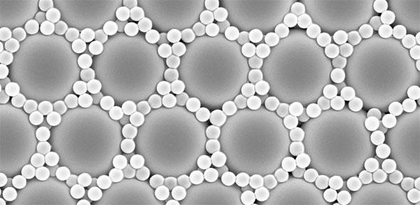
By controlling the nanoscale structure of solar cells made from these alternative materials, it is hoped that their efficiencies can be improved. The specific nanoscale structure shown in the video is a synthetic opal, a periodic pattern of closely packed spheres, the smallest of which are only 500 nm wide. By carefully controlling the drying of these spheres from water, they can be driven to self-assemble into this opal pattern. The resultant opal can then be used as a template for fabricating nanostructured solar cells.”

The polystyrene spheres shown in the image have two diameter sizes, the larger spheres are 3 μm across and the smaller spheres are 500 nm across. The image was taken using a scanning electron microscope at the Nanoscience Centre, University of Cambridge, with thanks to Professor Ullrich Steiner, the NanoDTC and EPSRC grant EP/G037221/1.

'Nanomaterials Up Close' is a special series linked to our 'Under the Microscope' collection of videos produced by Cambridge University that show glimpses of the natural and man-made world in stunning close-up.

In this video we see a synthetic opal, which is made using polystyrene spheres surrounded by even tinier polystyrene spheres around 1,000 times smaller than the width of a human hair. Harry Beeson, from the University of Cambridge, explains how it’s important to look at nanoscale structures like this to improve the efficiency of solar cells.

By carefully controlling the drying of these spheres from water, they can be driven to self-assemble into this opal pattern
Harry Beeson
Synthetic opal

The text in this work is licensed under a Creative Commons Licence. If you use this content on your site please link back to this page. For image rights, please see the credits associated with each individual image.
Yes
News type: 

Superconducting secrets solved after 30 years

$
0
0

Harnessing the enormous technological potential of high-temperature superconductors – which could be used in lossless electrical grids, next-generation supercomputers and levitating trains – could be much more straightforward in future, as the origin of superconductivity in these materials has finally been identified.

Superconductors, materials which can carry electric current with zero resistance, could be used in a huge range of applications, but a lack of understanding about where their properties originate from has meant that the process of identifying new materials has been rather haphazard.

Researchers from the University of Cambridge have found that ripples of electrons, known as charge density waves or charge order, create twisted ‘pockets’ of electrons in these materials, from which superconductivity emerges. The results are published in the June 15th issue of the journal Nature.

Low-temperature, or conventional, superconductors were first identified in the early 20th century, but they need to be cooled close to absolute zero (zero degrees on the Kelvin scale, or -273 degrees Celsius) before they start to display superconductivity. So-called high-temperature superconductors however, can display the same properties at temperatures up to 138 Kelvin (-135 degrees Celsius), making them much more suitable for practical applications.

Since they were first identified in the mid-1980s, the process of discovering new high-temperature superconductors could be best described as random. While researchers have identified the ingredients that make for a good low-temperature superconductor, high-temperature superconductors have been more reluctant to give up their secrets.

In a superconductor, as in any electronic device, current is carried via the charge on an electron. What is different about superconductors is that the electrons travel in tightly bound pairs. When travelling on their own, electrons tend to bump into each other, resulting in a loss of energy. But when paired up, the electrons move smoothly through a superconductor’s structure, which is why superconductors can carry current with no resistance. As long as the temperature is kept sufficiently low, the electron pairs will keep moving through the superconductor indefinitely.

Key to conventional superconductors are the interactions of electrons with the lattice structure of the material. These interactions generate a type of ‘glue’ which holds the electrons together. The strength of the glue is directly related to the strength of the superconductor, and when the superconductor is exposed to an increase in temperature or magnetic field strength, the glue is weakened, the electron pairs break apart and superconductivity is lost.

“One of the problems with high-temperature superconductors is that we don’t know how to find new ones, because we don’t actually know what the ingredients are that are responsible for creating high-temperature superconductivity in the first place,” said Dr Suchitra Sebastian of the Cavendish Laboratory, lead author of the paper. “We know there’s some sort of glue which causes the electrons to pair up, but we don’t know what that glue is.”

In order to decode what makes high-temperature superconductors tick, the researchers worked backwards: by determining what properties the materials have in their normal, non-superconducting state, they might be able to figure out what was causing superconductivity.

“We’re trying to understand what sorts of interactions were happening in the material before the electrons paired up, because one of those interactions must be responsible for creating the glue,” said Dr Sebastian. “Once the electrons are already paired up, it’s hard to know what made them pair up. But if we can break the pairs apart, then we can see what the electrons are doing and hopefully understand where the superconductivity came from.”

Superconductivity tends to override other properties. For example, if in its normal state a superconductor was a magnet, suppressing that magnetism has been found to result in superconductivity. “So by determining the normal state of a superconductor, it would make the process of identifying new ones much less random, as we’d know what sorts of materials to be looking for in the first place,” said Dr Sebastian.

Working with extremely strong magnetic fields, the researchers were able to kill the superconducting effect in cuprates - thin sheets of copper and oxygen separated by more complex types of atoms.

Previous attempts to determine the origins of superconductivity by determining the normal state have used temperature instead of magnetic field to break the electron pairs apart, which has led to inconclusive results.

As cuprates are such good superconductors, it took the strongest magnetic fields in the world – 100 Tesla, or roughly one million times stronger than the Earth’s magnetic field – in order to suppress their superconducting properties.

These experiments were finally able to solve the mystery surrounding the origin of pockets of electrons in the normal state that pair to create superconductivity. It was previously widely held that electron pockets were located in the region of strongest superconductivity. Instead, the present experiments using strong magnetic fields revealed a peculiar undulating twisted pocket geometry -similar to Jenga bricks where each layer goes in a different direction to the one above or beneath it.

These results pinpointed the pocket locations to be where superconductivity is weakest, and their origin to be ripples of electrons known as charge density waves, or charge order. It is this normal state that is overridden to yield superconductivity in the family of cuprate superconductors studied.

“By identifying other materials which have similar properties, hopefully it will help us find new superconductors at higher and higher temperatures, even perhaps materials which are superconductors at room temperature, which would open up a huge range of applications,” said Dr Sebastian.

A breakthrough has been made in identifying the origin of superconductivity in high-temperature superconductors, which has puzzled researchers for the past three decades.

By identifying other materials which have similar properties, hopefully it will help us find new superconductors at higher and higher temperatures
Suchitra Sebastian
Map of superconducting copper oxide structure.

The text in this work is licensed under a Creative Commons Licence. If you use this content on your site please link back to this page. For image rights, please see the credits associated with each individual image.

Yes
News type: 

Trapping the light fantastic

$
0
0

Jeremy Baumberg and his 30-strong team of researchers are master manipulators of light. They are specialists in nanophotonics – the control of how light interacts with tiny chunks of matter, at scales as small as a billionth of a metre. It’s a field of physics that 20 years ago was unknown.

At the heart of nanophotonics is the idea that changing the structure of materials at the scale of a few atoms can be used to alter not only the way light interacts with the material, but also its functional properties.

“The goal is to design materials with really intricate architecture on a really small scale, so small it’s smaller than the wavelength of light,” said Baumberg, Professor of Nanophotonics in the Department of Physics. “Whether the starting material is polystyrene or gold, changing the shape of its nanostructure can give us extraordinary control over how light energy is absorbed by the electrons locked inside. We’re learning how to use this to develop new functionality.”

One of their recent achievements is to develop synthetic materials that mimic some of nature’s most striking colours, among them the iridescent hue of opals. Naturally occurring opals are formed

‘Polymer opals’, however, are plastic – like the polystyrene in drinking cups – and formed within a matter of minutes. With some clever chemistry, the researchers have found a way of making polysterene spheres coated in a soft chewing-gum-like outer shell.

As these polymer opals are twisted and stretched, ‘metallic’ blue–green colours ripple across their surface. Their flexibility and the permanence of their intense colour make them ideal materials for security cards and banknotes or to replace toxic dyes in the textile industry.

“The crucial thing is that by assembling things in the right way you get the function you want,” said Baumberg, who developed the polymer opals with collaborators in Germany (at the DKI, now the Fraunhofer Institute for Structural Durability and System Reliability). “If the spheres are random, the material looks white or colourless, but if stacked perfectly regularly you get colour. We’ve found that smearing the spheres against each other magically makes them fall into regular lines and, because of the chewing gum layer, when you stretch it the colour changes too.

“It’s such a good example of nanotechnology – we take a transparent material, we cut it up in the right form, we stack it in the right way and we get completely new function.”

Although nanophotonics is a comparatively new area of materials research, Baumberg believes that within two decades we will start to see nanophotonic materials in anything from smart textiles to buildings and food colouring to solar cells.

Now, one of the team’s latest discoveries looks set to open up applications in medical diagnostics.

“We’re starting to learn how we can make materials that respond optically to the presence of individual molecules in biological fluids,” he explained. “There’s a large demand for this. GPs would like to be able to test the patient while they wait, rather than sending samples away for clinical testing. And cheap and reliable tests would benefit developing countries that lack expensive diagnostic equipment.”

A commonly used technique in medical diagnostics is Raman spectroscopy, which detects the presence of a molecule by its ‘optical signature’. It measures how light is changed when it bounces off a molecule, which in turn depends on the bonds within the molecule. However, the machines need to be very powerful to detect what can be quite weak effects.

Baumberg has been working with Dr Oren Scherman, Director of the Melville Laboratory for Polymer Synthesis in the Department of Chemistry, on a completely new way to sense molecules they have developed using a barrel-shaped molecular container called cucurbituril (CB). Acting like a tiny test tube, CB enables single molecules to enter its barrel shape, effectively isolating them from a mixture of molecules.

In collaboration with researchers in Spain and France, and with funding from the European Union, Baumberg and Scherman have found a way to detect what’s in each barrel using light, by combining the barrels with particles of gold only a few thousand atoms across.

“Shining light onto this gold–barrel mixture focuses and enhances the light waves into tiny volumes of space exactly where the molecules are located,” Baumberg explained. “By looking at the colours of the scattered light, we can work out which molecules are present and what they are doing, and with very high sensitivity.”

Whereas most sensing equipment requires precise conditions that can only really be achieved in the laboratory, this new technology has the potential to be a low-cost, reliable and rapid sensor for mass markets. The amount of gold required for the test is extremely small, and the gold particles self-assemble with CB at room temperature.

Now, with funding from the Engineering and Physical Sciences Research Council, and working with companies and potential end users (including the NHS), Baumberg and Scherman have begun the process of developing their ‘plasmonic sensors’ to test biological fluids such as urine and tears, for uses such as detecting neurotransmitters in the brain and protein incompatibilities between mother and fetus.

“At the same time, we want to understand how we can go further with the technology, from controlling chemical reactions happening inside the barrel, to making captured molecules inside ‘flex’ themselves, and detecting each of these modifications through colour change,” added Baumberg.

“The ability to look at small numbers of molecules in a sea of others has appealed to scientists for years. Soon we will be able to do this on an unprecedented scale: watching in real time how molecules come together and undergo chemical reactions, and even how they form a bond. This has huge implications for optimising catalysis in industrially relevant processes and is therefore at the heart of almost every product in our lives.”

Baumberg views nanophotonics technology as a whole new toolbox. “The excitement for me is the challenge of how difficult the task is combined with the fact that you can see that, if only you could do it, you can get things out that are incredible.

“At the moment we are capable of assembling new structures with different optical properties in a highly controlled way. Eventually, though, we will be able to build things with light itself.”

The development of a ‘nanobarrel’ that traps and concentrates light onto single molecules could be used as a low-cost and reliable diagnostic test.

Eventually... we will be able to build things with light itself
Jeremy Baumberg
Light can be manipulated at the nanoscale, as in this elastic material which has been folded like nano-origami

The text in this work is licensed under a Creative Commons Licence. If you use this content on your site please link back to this page. For image rights, please see the credits associated with each individual image.

Yes
News type: 

The atomic building site

$
0
0

Making a perfectly flat layer of billiard balls is fairly straightforward. Doing the same thing with atoms is rather more difficult. But as we demand more of materials, the ability to control atoms as if they were billiard balls is required to make the next generation of advanced materials possible.

Researchers in Cambridge are bringing these ‘made-to-measure’ materials one step closer to practical applications, and soon they will do so at unprecedented levels, thanks to a new pulsed laser deposition (PLD) system – unique in the UK – that allows for atom-by-atom design and growth.

Oxides are prime candidates for making these new applications possible. Complex oxides – compounds of oxygen and one or more metallic elements – potentially have new properties that surpass those of silicon-based electronics. These make them ideal for next-generation computing devices that process vast amounts of data in an energy-efficient way.

However, it’s extremely difficult to control the growth of complex oxides at the atomic level. To achieve this, new methods of laying down atoms need to be found, and any defects in the materials need to be minimised or eliminated.

Defects influence the electronic properties of a material. In conventional electronic devices, information is carried via the charge or spin on electrons, so anything interfering with the electrons will affect the material’s performance. Atoms located in the wrong place or missing entirely can snare electrons like a mouse in a trap. The number of defects that can be tolerated varies depending on the application. Semiconductors, for instance, need to be as close to perfection as possible: the maximum amount of imperfection that can be tolerated is roughly equivalent to a pinhead on a football pitch.

“Designing and growing new materials at the atomic scale are not yet ‘made-to-measure’ processes,” said Professor Judith Driscoll of the Department of Materials Science and Metallurgy, who specialises in fine-tuning the properties of oxides for applications in energy, low-energy electronics and photovoltaics. The properties of oxide materials can be manipulated by changing the bond lengths or angles between atoms, but cost-effectively designing them to be as close to perfect as possible is not easy.

“Over the past 15 years, we’ve made huge advances with making materials perfect at nanometre-length scales, but we still can’t easily understand things going on at the atomic scale. You assume that things are perfect, but in reality they are not, and you don’t know by how much – you can only infer it from indirect measurements. To make really perfect structures, you have to be able to control the number of atoms being deposited and to stop at the exact point that a single complete layer has been grown.”

Most metal oxides are grown using thin-film deposition techniques, where atomic layers are built one on top of the other on a substrate. Thin-film techniques are used by several Cambridge research groups who are interested in the physics and chemistry of functional materials, and how they can be manipulated. For instance, in the Department of Physics, researchers are using these techniques to explore the quantum properties of semiconductors. In Materials Science, Professor Neil Mathur’s group uses thin films to study the electrical and magnetic properties of materials, for example attempting to control either their temperature or their magnetism through voltage; and Professor Mark Blamire’s group is using them to create new kinds of magnetic and superconducting devices.

While thin-film techniques such as ‘sputtering’ (eroding material from a source onto a substrate) have been vital in getting advanced materials such as metal oxides to their current state, they do not provide either the level of control that’s needed to see them used in practical applications nor the capabilities to make them at scale, as Blamire explained: “Sputtering is a very flexible and accurate technique for many types of metals, but it is not particularly well-suited to single-crystal oxide thin films. We have invested heavily in pulsed laser deposition, but the thickness control and the range of materials which can be grown is still limited.”

Now, Driscoll, along with colleagues in Materials Science and the Department of Physics, has secured funding from the University and the Engineering and Physical Sciences Research Council for state-of-the-art new PLD equipment that will make ‘made-to-measure’ materials possible. The new system uses advanced PLD with reflective high-energy electron diffraction to control growth rate and produce single atomic layers with a minimum of defects.

The technique will give researchers the capability to measure thin-film thicknesses with extremely high levels of accuracy – down to less than one nanometre in thickness – as well as the ability to perform in situ chemical analysis to ensure the materials and the surfaces they are creating have the intended chemical and electronic structures.

“In addition to helping us build really useful things from oxides, this new technology will help us to discover and explore the properties of new materials,” added Driscoll. “It will take some long-term thinking to see them transition to practical applications, but once we achieve control over these materials at the atomic scale, the practical applications will follow. We believe that such oxides could really revolutionise electronics.”

The ability to design, control and build new materials at the level of individual atoms could open up a whole new world of electronic devices.

This new technology will help us to discover and explore the properties of new materials
Judith Driscoll
Atomium

The text in this work is licensed under a Creative Commons Licence. If you use this content on your site please link back to this page. For image rights, please see the credits associated with each individual image.

Yes
News type: 

Black hole trio holds promise for gravity wave hunt

$
0
0

An international team, including University of Cambridge scientists, led by Dr Roger Deane from the University of Cape Town, examined six systems thought to contain two supermassive black holes. The team found that one of these contained three supermassive black holes – the tightest trio of black holes detected at such a large distance – with two of them orbiting each other rather like binary stars. The finding suggests that these closely-packed supermassive black holes are far more common than previously thought.

A report of the research is published in this week’s Nature.

Dr Roger Deane from the University of Cape Town said: ‘What remains extraordinary to me is that these black holes, which are at the very extreme of Einstein’s Theory of General Relativity, are orbiting one another at 300 times the speed of sound on Earth. Not only that, but using the combined signals from radio telescopes on four continents we are able to observe this exotic system one third of the way across the Universe. It gives me great excitement as this is just scratching the surface of a long list of discoveries that will be made possible with the Square Kilometre Array (SKA).’

The team used a technique called Very Long Baseline Interferometry (VLBI) to discover the inner two black holes of the triple system. This technique combines the signals from large radio antennas separated by up to 10,000 kilometres to see detail 50 times finer than that possible with the Hubble Space Telescope. The discovery was made with the European VLBI Network, an array of European, Chinese, Russian and South African antennas, as well as the 305 metre Arecibo Observatory in Puerto Rico. Future radio telescopes such as the SKA will be able to measure the gravitational waves from such black hole systems as their orbits decrease.

At this point, very little is actually known about black hole systems that are so close to one another that they emit detectable gravitational waves. According to Prof Matt Jarvis from the Universities of Oxford and the Western Cape, ‘This discovery not only suggests that close-pair black hole systems emitting at radio wavelengths are much more common than previously expected, but also predicts that radio telescopes such as MeerKAT and the African VLBI Network (AVN, a network of antennas across the continent) will directly assist in the detection and understanding of the gravitational wave signal. Further in the future the SKA will allow us to find and study these systems in exquisite detail, and really allow us gain a much better understanding of how black holes shape galaxies over the history of the Universe.’

Dr Keith Grainge of the University of Manchester, an author of the paper, said: ‘This exciting discovery perfectly illustrates the power of the VLBI technique, whose exquisite sharpness of view allows us to see deep into the hearts of distant galaxies. The next generation radio observatory, the SKA, is being designed with VLBI capabilities very much in mind.’

While the VLBI technique was essential to discover the inner two black, the team has also shown that the binary black hole presence can be revealed by much larger scale features. The orbital motion of the black hole is imprinted onto its large jets, twisting them into a helical or corkscrew-like shape. So even though black holes may be so close together that our telescopes cannot tell them apart, their twisted jets may provide easy-to-find pointers to them, much like using a flare to mark your location at sea. Indeed, the high radio frequency Arcminute Microkelvin Imager (AMI) telescope at Cambridge, used in the paper, shows emission from this black-hole system that increases at high frequency, a phenomenon directly due to extremely compact jets yet with relativistic speeds. This may provide sensitive future telescopes like MeerKAT and the SKA a way to find binary black holes with much greater efficiency.

The discovery of three closely orbiting supermassive black holes in a galaxy more than four billion light years away could help astronomers in the search for gravitational waves: the ‘ripples in spacetime’ predicted by Einstein.

This exciting discovery perfectly illustrates the power of the VLBI technique, whose exquisite sharpness of view allows us to see deep into the hearts of distant galaxies.
Dr Keith Grainge
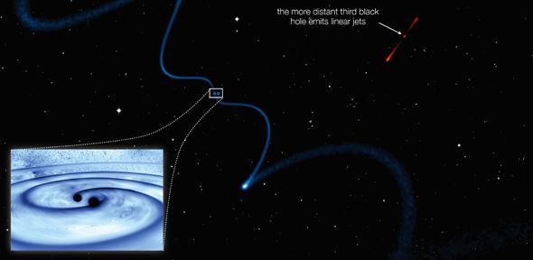
Helical jets from one supermassive black hole caused by a very closely orbiting companion (see blue dots). The third black hole is part of the system, but farther away and therefore emits relatively straight jets.

The text in this work is licensed under a Creative Commons Licence. If you use this content on your site please link back to this page. For image rights, please see the credits associated with each individual image.
Yes
News type: 

Light in, light out: the ‘rock’ that breaks the rules

$
0
0

Discovered 175 years ago in Russia’s mineral treasure box – the Ural Mountains – and named after the mineralogist Count Lev Aleksevich von Perovski, perovskite is fast becoming a ‘rock’ to be reckoned with. In 2013, the use of perovskite materials in solar cells was voted as one of the breakthroughs of the year by Sciencemagazine; more recently, the Guardianwebsite declared that they “are the clean tech material development to watch right now.”

Perovskite is a term used to describe a group of materials that have a distinctive crystal structure of cuboid and diamond shapes. They have long been of interest for their superconducting and ferroelectric properties. But, in the past five years, it was discovered that they are also remarkably efficient at absorbing photons of light and that this can be converted into an electric current in photovoltaic solar cells.

A defining moment came in 2012, when Professors Henry Snaith at the University of Oxford and Michael Graetzel at the Federal Institute of Technology Lausanne, building on the work of Tsotomu Mayasaka from Tokyo, found that solar cells with perovskite as the active component could be made with greater than 10% power conversion efficiencies for turning the sun’s rays into electrical energy. A mere two years later, Snaith increased this to 17%. For silicon-based solar cells, it’s taken 20 years of research to achieve this level.

Now, researchers in Cambridge have found another property of this remarkable material – it doesn’t just absorb light, it also emits it as a laser.

Led by Professor Sir Richard Friend from the Department of Physics, the researchers have been investigating how perovskites work by exciting the material with light and monitoring energy absorption at incredibly fast timescales, taking ‘snapshots’ a few quadrillionths of a second apart.

As PhD student Michael Price described: “This enables us to monitor directly what is happening to the electrons, which generate the current in the material – where the excitations are and how they are destroyed, essentially how fast they live and die.”

In collaboration with Snaith’s group in Oxford, the scientists are using this fundamental insight to help them understand how the efficiency of perovskite-based photovoltaics might be extended yet further.

The lasing properties (published in the Journal of Physical Chemistry Letters in March) were discovered when Friend’s team measured the photoluminescence efficiency of the material, and found that up to 70% of absorbed photons were emitted under the right conditions. This led to the idea of sandwiching a thin layer of the lead halide perovskite between two mirrors to create an optically driven laser.

“It turns out that perovskites are remarkably fluorescent materials,” explained Friend. This is not in itself a surprise – since the early 1960s a relationship between the generation of electrical charges following light absorbtion and the process of ‘recombination’ of these charges to emit light has been known. “But these materials do so very efficiently,” said Friend. “It’s unusual in a material that is so simply and cheaply prepared.”

“Mix and squirt,” is how Price described the preparation process: “we make a solution of the halide perovskites and spin- coat them onto an electrode. There’s no need for elaborate purification.” This simple process, which the scientists say is scalable, is in contrast to the painstaking growth of crystals needed for other solar cell materials like silicon to ensure that the number of defects in the materials is kept as low as possible.

“Perovskites are cheap and abundant, they are easily fabricated and they have a high efficiency of energy conversion – these three together are the holy grail of photovoltaics, which is why there is such excitement about them at the moment,” added Dr Felix Deschler.

The lasing properties of perovskites raise expectations for even higher solar cell efficiencies, as Friend explained: “There’s a fundamental relationship between how good a material is at emitting light and how well it works in a solar cell.”

The team’s work is based on a programme of research on organic (i.e. carbon-containing) semiconductors that has spanned over 20 years in Friend’s laboratory, most recently as part of the Winton Programme for the Physics of Sustainability, and has resulted in the development of roll-to-roll printing of photovoltaic materials, light-emitting diodes (LEDs) and printed transistors for paper displays. The techniques Friend’s group has developed for characterising organic semiconductors are now being deployed on the mostly inorganic perovskite materials.

The current focus is on identifying the fundamental mechanisms that are at play when photons of light raise electrons in the material to higher energy states, and on looking at precisely how and where energy losses occur – an understanding of which will be crucial to maximising the efficiency of these light-harvesting solar cells.

Intriguingly, early results show that the material doesn’t appear to work in the way that might be expected. “For me, the excitement is that these materials break the rules,” said Friend. “Many of their properties are somewhere between those of an organic and an inorganic semiconductor. The way we make them, they should have too many chemical and structural defects to work as well as they do and yet they are as efficient as purified silicon, which is a single crystal.”

Would they be better if cleaned up? “Possibly,” said Friend, “but we want to have our cake and eat it. We want the efficiencies and the ease of preparation.”

Defects in materials normally cause charged electrons to get ‘stuck’ and lose their energy. One possibility for perovskites might be that the defects don’t matter because the material has the capacity to ‘self-heal’.

“There’s something going on... these materials have a tolerance to disorder
which is unusual,” explained Friend. “It’s speculation, but perhaps the material can fill defects on the fly. The way the material is prepared creates a lot of free ions, and these might move around and fill up defects. Imagine a bumpy road with potholes – the ions might fill the potholes and then the electrons have a smooth ride.”

A better understanding of these processes will feed into the collaboration with Snaith’s group, helping the scale-up and commercial deployment of perovskite-based photovoltaics through the Oxford spin-out Oxford Photovoltaics.

Meanwhile, the Cambridge team is also pursuing the material’s light-emitting properties, as Deschler explained: “It opens up a completely new field of applications. The laser industry is huge – they are used in areas that are critical for our lives, including telecommunications, medicine and industry. We think there will be applications for perovskites that extend far beyond thesolar cell.”

In particular, the researchers are now looking at applying the high luminescence efficiency to create light-emitting diodes. Other members in the research group have already had some very promising results in this area, which should be published soon.

“This feels like it’s the dawn of a new field,” said Friend. “So far we’ve looked at the materials as they are. The question now is how good will they be?”

Perovskite materials are the newest contender for breaking the silicon ceiling in solar cell technology. But they don’t just absorb light. Cambridge researchers have found they emit it like a laser, opening up an entirely new field of applications.

This feels like it’s the dawn of a new field. So far we’ve looked at the materials as they are. The question now is how good will they be?
Professor Sir Richard Friend

The text in this work is licensed under a Creative Commons Licence. If you use this content on your site please link back to this page. For image rights, please see the credits associated with each individual image.

Yes
News type: 

Nanomaterials Up Close: Gum Arabic

$
0
0

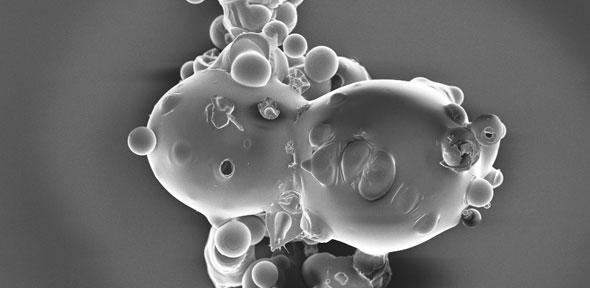
"This lustrous picture was taken on an electron microscope, allowing us to see below the wavelength of light. It's actually a very boring scrap of gum arabic powder, which is made from the hardened sap of the Acacia tree, probably collected in Sudan.

Gum arabic is a common additive in food, glue and polish where it works as a thickener and emulsifier.

By covering it in a nanoscale layer of gold, and bombarding it with electrons in a vacuum, we reveal its smooth and alien texture, and the beauty hidden in this plain speck of dust.

We can learn a lot from looking at structures in natural materials at this very small scale. They tells us how we can adapt them to build our own new materials with new characteristics and uses.”

This image was taken while Rox was doing a summer placement with Alex Finnemore in the Thin Films and Interfaces group using the SEM in the Nanoscience Centre. Rox is currently a student in the NanoDTC.

'Nanomaterials Up Close' is a special series linked to our 'Under the Microscope' collection of videos produced by Cambridge University that show glimpses of the natural and man-made world in stunning close-up.

This alien glob is a piece of gum arabic from the hardened sap of the Acacia tree, most likely collected from a tree in Sudan. Rox Middleton explains how the electron microscope has changed the way we are able to interact with objects at the nanoscale, allowing us to enjoy a glimpse of the exquisite abstract forms around us.

We reveal its smooth and alien texture, and the beauty hidden in this plain speck of dust
Rox Middleton
Gum Arabic

The text in this work is licensed under a Creative Commons Licence. If you use this content on your site please link back to this page. For image rights, please see the credits associated with each individual image.

Yes
News type: 

Institute of Physics announces 2014 award winners

$
0
0

The Institute of Physics (IOP) has announced this year’s award winners with three Cambridge academics among their ranks.

In its Gold award category is Professor Michael Payne from University of Cambridge receiving the Swan Medal “for the development of computational techniques that have revolutionised materials design and facilitated the industrial application of quantum mechanical simulations”.

The Swan Medal is given for outstanding contributions to the organisation or application of physics in an industrial or commercial context.

Professor Benjamin Simons received the The IOP’s Franklin Medal and Prize, which is a Subject award given for distinguished research in physics applied to the life sciences including medical and biological physics.

The citation read: “For the application of non-equilibrium statistical mechanic to provide fundamental new insights into the mechanisms that regulate stem cell behaviour in tissue maintenance and disease”.

Recognised with the Paterson Medal and Prize – given for distinguished early career research in applied physics - was Dr Sarah Bohndiek

The citation read: “For her remarkable work in developing advanced molecular imaging techniques and applying them to address questions at the interface of physics, biology and medicine.”

The full list of award winners, including early career, education and outreach awards, can be found at www.iop.org/awards.

Physics awards honour work of Cambridge academics

The text in this work is licensed under a Creative Commons Licence. If you use this content on your site please link back to this page. For image rights, please see the credits associated with each individual image.
Yes
News type: 

"Brain Workout" for Physics Teachers at the Cavendish Laboratory

$
0
0

Funded by the Rutherford Physics Partnership, the residential has been held for four years alongside the Senior Physics Challenge.

The residential provides teachers with copies of the resources and ideas which underpin the Rutherford Physics Project and the Senior Physics Challenge, so that they can take them back to school and into their classrooms, and the opportunity to see how the students taking part in the Challenge tackle the problems.

“It can be really difficult to find things for our higher-level physics students to do,” said Holly Lindsay, Head of Physics at Ormiston Sudbury Academy, Suffolk.

“This residential has provided lots of resources and two really good websites which I can use with our top physicists.”

“It’s also been a great opportunity for networking – we’ve been sharing our emails and are going to carry on sharing ideas when we get back into the classroom,” Holly added.

The residential also gives teachers the opportunity to discuss physics and physics education with each other and with Cambridge academics, and a chance to think in alternative ways about teaching.

John Crossland, Science Teacher at Beaminster School, has travelled from Dorset to join the residential.

“It’s been really invaluable – it’s going to really help me add value to teaching our Gifted and Talented A Level students," John said.

“We’ve been hearing about the plans for the Rutherford Physics Partnership MOOC – it’s really exciting that these resources will be available for me to use as extension activities, and that our more able and talented physicists will have somewhere to go to challenge their brains.

“The insight into the course provision at Cambridge and the requirements to gain entry into the university have also been an eye-opener for me.”

"Because we’ve been visiting and staying in the different Colleges, I feel like I’ve had a good chance to see what it would be like to attend Cambridge as an undergraduate.”

The Rutherford Physics Project is a five-year project, that began in 2013, aimed at developing the skills of sixth-form physicists  (funded by a £7 million grant by the Department for Education) which is delivering extension materials, on-line learning, workshops for students and support for physics teachers. 

“Our hope and goal is that the learning resources and activities offered by the project will enable more students from all backgrounds to gain physics expertise beyond school level, encourage more students to apply for physics, engineering and mathematics at highly-selective universities throughout the UK, and equip them to best demonstrate their academic potential,” said Dr. Lisa Jardine Wright, co-director of the Rutherford Physics Project.

“The residential is also an opportunity for the Faculty to discuss ideas and concepts with teachers. Teachers know the areas of the curriculum which students find challenging. Their assistance in developing our Rutherford Physics Project resources is invaluable,” she added.

“It’s a proper brain workout,” said one of the thirty-seven physics teachers enjoying three days of subject workshops, practical experiments and teaching observations at the Physics Teachers Cambridge Residential.

Science Teachers carry out experiments in the Cavendish Laboratory

The text in this work is licensed under a Creative Commons Licence. If you use this content on your site please link back to this page. For image rights, please see the credits associated with each individual image.

Yes
News type: 

Building ‘invisible’ materials with light

$
0
0

A new method of building materials using light, developed by researchers at the University of Cambridge, could one day enable technologies that are often considered the realm of science fiction, such as invisibility cloaks and cloaking devices.

Although cloaked starships won’t be a reality for quite some time, the technique which researchers have developed for constructing materials with building blocks a few billionths of a metre across can be used to control the way that light flies through them, and works on large chunks all at once. Details are published today (28 July) in the journal Nature Communications.

The key to any sort of ‘invisibility’ effect lies in the way light interacts with a material. When light hits a surface, it is either absorbed or reflected, which is what enables us to see objects. However, by engineering materials at the nanoscale, it is possible to produce ‘metamaterials’: materials which can control the way in which light interacts with them. Light reflected by a metamaterial is refracted in the ‘wrong’ way, potentially rendering objects invisible, or making them appear as something else.

Metamaterials have a wide range of potential applications, including sensing and improving military stealth technology. However, before cloaking devices can become reality on a larger scale, researchers must determine how to make the right materials at the nanoscale, and using light is now shown to be an enormous help in such nano-construction.

The technique developed by the Cambridge team involves using unfocused laser light as billions of needles, stitching gold nanoparticles together into long strings, directly in water for the first time. These strings can then be stacked into layers one on top of the other, similar to Lego bricks. The method makes it possible to produce materials in much higher quantities than can be made through current techniques.

In order to make the strings, the researchers first used barrel-shaped molecules called cucurbiturils (CBs). The CBs act like miniature spacers, enabling a very high degree of control over the spacing between the nanoparticles, locking them in place.

In order to connect them electrically, the researchers needed to build a bridge between the nanoparticles. Conventional welding techniques would not be effective, as they cause the particles to melt. “It’s about finding a way to control that bridge between the nanoparticles,” said Dr Ventsislav Valev of the University’s Cavendish Laboratory, one of the authors of the paper. “Joining a few nanoparticles together is fine, but scaling that up is challenging.”

The key to controlling the bridges lies in the cucurbiturils: the precise spacing between the nanoparticles allows much more control over the process. When the laser is focused on the strings of particles in their CB scaffolds, it produces plasmons: ripples of electrons at the surfaces of conducting metals. These skipping electrons concentrate the light energy on atoms at the surface and join them to form bridges between the nanoparticles. Using ultrafast lasers results in billions of these bridges forming in rapid succession, threading the nanoparticles into long strings, which can be monitored in real time.

“We have controlled the dimensions in a way that hasn’t been possible before,” said Dr Valev, who worked with researchers from the Department of Chemistry, the Department of Materials Science & Metallurgy, and the Donostia International Physics Center in Spain on the project. “This level of control opens up a wide range of potential practical applications.”

A new technique which uses light like a needle to thread long chains of particles could help bring sci-fi concepts such as cloaking devices one step closer to reality.

This level of control opens up a wide range of potential practical applications
Ventsislav Valev
An efficient route to manufacturing nanomaterials with light through plasmon-induced laser-threading of gold nanoparticle strings

The text in this work is licensed under a Creative Commons Licence. If you use this content on your site please link back to this page. For image rights, please see the credits associated with each individual image.
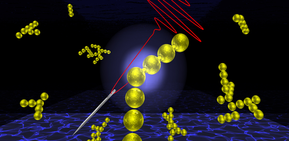
Yes

LEDs made from ‘wonder material’ perovskite

$
0
0

A hybrid form of perovskite - the same type of material which has recently been found to make highly efficient solar cells that could one day replace silicon - has been used to make low-cost, easily manufactured LEDs, potentially opening up a wide range of commercial applications in future, such as flexible colour displays.

This particular class of semiconducting perovskites have generated excitement in the solar cell field over the past several years, after Professor Henry Snaith’s group at Oxford University found them to be remarkably efficient at converting light to electricity. In just two short years, perovskite-based solar cells have reached efficiencies of nearly 20%, a level which took conventional silicon-based solar cells 20 years to reach.

Now, researchers from the University of Cambridge, University of Oxford and the Ludwig-Maximilians-Universität in Munich have demonstrated a new application for perovskite materials, using them to make high-brightness LEDs. The results are published in the journal Nature Nanotechnology.

Perovskite is a general term used to describe a group of materials that have a distinctive crystal structure of cuboid and diamond shapes. They have long been of interest for their superconducting and ferroelectric properties. But in the past several years, their efficiency at converting light into electrical energy has opened up a wide range of potential applications.

The perovskites that were used to make the LEDs are known as organometal halide perovskites, and contain a mixture of lead, carbon-based ions and halogen ions known as halides. These materials dissolve well in common solvents, and assemble to form perovskite crystals when dried, making them cheap and simple to make.

“These organometal halide perovskites are remarkable semiconductors,” said Zhi-Kuang Tan, a PhD student at the University of Cambridge’s Cavendish Laboratory and the paper’s lead author. “We have designed the diode structure to confine electrical charges into a very thin layer of the perovskite, which sets up conditions for the electron-hole capture process to produce light emission.”

The perovskite LEDs are made using a simple and scalable process in which a perovskite solution is prepared and spin-coated onto the substrate. This process does not require high temperature heating steps or a high vacuum, and is therefore cheap to manufacture in a large scale. In contrast, conventional methods for manufacturing LEDs make the cost prohibitive for many large-area display applications.

“The big surprise to the semiconductor community is to find that such simple process methods still produce very clean semiconductor properties, without the need for the complex purification procedures required for traditional semiconductors such as silicon,” said Professor Sir Richard Friend of the Cavendish Laboratory, who has led this programme in Cambridge.

“It’s remarkable that this material can be easily tuned to emit light in a variety of colours, which makes it extremely useful for colour displays, lighting and optical communication applications,” said Tan. “This technology could provide a lot of value to the ever growing flat-panel display industry.”

The team is now looking to increase the efficiency of the LEDs and to use them for diode lasers, which are used in a range of scientific, medical and industrial applications, such as materials processing and medical equipment. The first commercially-available LED based on perovskite could be available within five years.

Colourful LEDs made from a material known as perovskite could lead to LED displays which are both cheaper and easier to manufacture in future.

This technology could provide a lot of value to the ever growing flat-panel display industry
Zhi-Kuang Tan
LEDs made from perovskite

The text in this work is licensed under a Creative Commons Licence. If you use this content on your site please link back to this page. For image rights, please see the credits associated with each individual image.

Yes
Viewing all 258 articles
Browse latest View live


Latest Images